Blog
PCB Terminology
List of proper PCB Terminology
Understanding these key PCB terminologies is crucial for effective communication, collaboration, and successful design and manufacturing of printed circuit boards.
PCB (Printed Circuit Board) Terminology:
- Trace: A conductive pathway on a PCB that carries electrical signals between components.
- Pad: A small area of copper on the PCB used for component soldering or connection points.
- Via: A plated hole that connects different layers of a PCB, allowing signals to pass through.
- SMD (Surface Mount Device): Components that are mounted directly onto the surface of a PCB using solder paste and reflow soldering techniques.
- Through-Hole Component: Components that have leads or pins that pass through holes in the PCB and are soldered on the other side.
- Silkscreen: The layer on the PCB that displays component outlines, reference designators, and other markings to assist with assembly and identification.
Silkscreening is a process used in printed circuit board (PCB) manufacturing to apply markings, labels, or symbols onto the PCB surface. It involves printing ink onto the PCB using a specialized machine called a silkscreen printer. The silkscreen layer is typically applied on the top and bottom sides of the PCB, and it helps identify components, reference designators, test points, logos, and other important information related to the board. - PCB Holes: There are typically two types of holes in PCB.
- Copper Pour: A large area of copper on the PCB used for providing a ground or power plane, reducing noise, or improving heat dissipation.
- Mask (Solder Mask): A protective layer applied to the PCB to insulate and prevent solder bridges between components and traces during soldering.
- Drill File: A file that contains the positions and sizes of holes drilled in the PCB for through-hole components or vias.
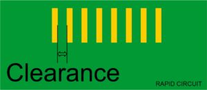
- Clearance: The minimum distance between two conductive traces, pads, or components to avoid electrical interference or short circuits.
- Annular Ring: The copper area surrounding a drilled hole, ensuring proper electrical connection between a pad or via and the corresponding layer.
- BOM (Bill of Materials): A list of components and their specifications required to assemble the PCB, including part numbers, quantities, and reference designators.
- DFM (Design for Manufacturability): Design practices and guidelines that ensure the PCB can be efficiently manufactured, assembled, and tested.
- DRC (Design Rule Check): A software-based check that verifies if the PCB design conforms to specific manufacturing rules, such as minimum trace width, clearance, and drill hole sizes.
- Impedance Control: The management and maintenance of specific electrical characteristics, such as impedance, to ensure signal integrity on high-speed or sensitive circuitry.
- ESD (Electrostatic Discharge): The sudden discharge of static electricity that can damage or destroy electronic components. ESD protection measures are incorporated into PCB designs to prevent such damage.
- Power Plane: A dedicated layer on a PCB that provides a continuous power distribution network for supplying power to components.
- Ground Plane: A layer on a PCB that serves as a reference point for electrical signals and provides a low-impedance return path for current flow.
- RoHS (Restriction of Hazardous Substances): A directive that restricts the use of certain hazardous substances, such as lead and mercury, in electronic products to promote environmental protection.
- PCB Holes: There are typically two types of holes in PCB.
- PTH: Plated thru-hole: PTH holes may be either component holes or vias. Component holes are for component assembly based on component dimensions. Via holes carry current from one layer to another layer.
- NPTH: Non-plated thru-hole: NPTH holes are for PCB mounting purposes. Standard mounting hole sizes are between 3 mm and 5 mm. PCB holes are made with drill bits, mostly on CNC drilling machines. Bigger mounting holes (6 mm or larger) are made with CNC routing machines.
- Annular ring: An annular ring is a copper area around the PTH hole and vias to ensure good connections in circuit boards.
- Pad: The copper area around the holes is called pads. Pads are in shapes like Round, Square, Rectangle, ovals, hexagons, octagons, etc. Copper points for SMD component assembly are called SMD pads. Generally, the SMD pad shape is square and rectangular. There are no holes in SMD pads.There may be a few points where reading has to be taken on Printed circuit boards. These points are called test pads. Generally, the test pad shape is round with silkscreen identification TP. Test points may be with or without holes.

- Trace or Track: A PCB trace or track is a copper conductor line that carries the signal from one pad to another or many pads.
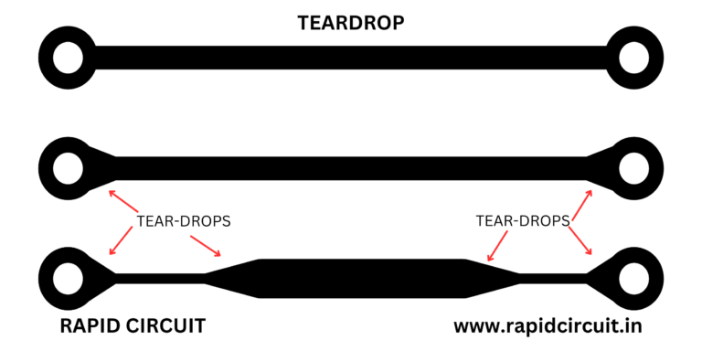
- Teardrop: A teardrop is an extra copper at a junction of traces and pads ( either with vias or components). Teardrops may be a straight or round shape. Teardrops are also used for trace transition. For example, when the trace width is reduced to 3 mils from 5 mils, the teardrop is added at the transition point to minimize cracks or stress.
- PCB Board Thickness
PCB (Printed Circuit Board) thickness can vary depending on the specific requirements of the application and the design considerations. However, standard PCBs typically have a thickness ranging from 0.4mm (0.016 inches) to 3.2mm (0.126 inches).
Thinner PCBs, such as those with a thickness of 0.4mm or 0.8mm, are commonly used in applications where space is a constraint, such as mobile devices or compact electronics. Thicker PCBs, such as 1.6mm or 2.0mm, are more common in general electronic devices.
It’s important to note that the PCB thickness can impact the overall mechanical stability, flexibility, and manufacturability of the board. Thicker PCBs offer greater rigidity and can handle higher component weights, while thinner PCBs provide flexibility and can be more suitable for certain applications.
Additionally, specialized PCBs can have custom thicknesses outside of the standard range mentioned above. These may include ultra-thin PCBs for specific requirements or thicker boards for applications that require extra durability or heat dissipation.
When designing a PCB, it’s essential to consider the electrical and mechanical requirements of the components, the board’s intended application, and any specific manufacturing guidelines provided by the PCB manufacturer.
- Copper Weight
Copper weight confirms the copper thickness on board. Hence copper weight is more important on PCB.
The current-carrying capacity on PCB depends on the thickness of the trace; hence, the higher the copper weight, the higher the current capacity.
1oz of copper is rolled out over an area of 1 square foot is 1oz copper weight, and in this case, copper thickness is 1.4 mils (or 0.035 mm or 35 microns)
Copper weight is measured and discussed in ounces per square foot (oz/ft²), and examples as below.
| Copper Weight (oz/ft²) | The copper thickness on board in mils | The copper thickness on board in mm | The copper thickness on board in microns |
| 0.5 oz | 0.7 mils | 0.018 mm | 18 microns |
| 1 oz | 1.4 mils | 0.035 mm | 35 microns |
| 2 oz | 2.8 mils | 0.070 mm | 70 microns |
Most PCBs are made up of 1 oz copper weight in the industry, and high-power PCBs are made up of 2 oz copper weight. Very few PCBs are made up of higher copper weight for special applications.
- PCB Outline
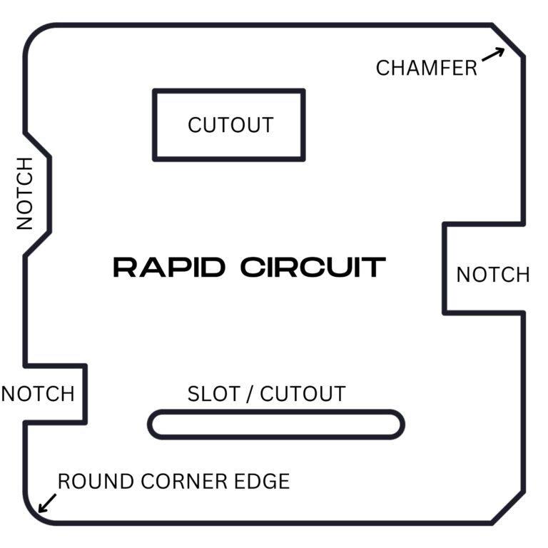
The printed circuit board’s outer border is called the outline. The outline is drawn with lines and arcs in designing software. PCB Outline is also called PCB board Profile.
PCB outline shape may be rectangle, square, round, or irregular.
- Cutout
Any regular or irregular shape cutting inside a PCB profile is called a cutout.
The cutout may be slots, rectangles, squares, round hole shapes and any other irregular shape.
The cutout may be plated or non-plated. ( most of the time non-platted)
A cutout is done using a routing bit ( also a router bit) on a CNC machine.
- PCB Notch
A printed circuit board with a cutout on the board profile is a PCB notch.
- Gerber file
The Gerber format is an open ASCII vector format for printed circuit board (PCB) designs. It is one of the most used PCB Terminology.
PCB houses need a Gerber to fabricate PCBs.
There are three types of Gerber.
- Extended Gerber (Gerber 274X or RS-274X) is a standard format common in the industry.
- Standard Gerber (Gerber-D or RS-274-D) is an old data format. The Gerber-D design requires a wheel file( or aperture file) to read the Dcode of all lines, pads, arcs, surfaces and texts.
- GerberX2: it is an Extended Gerber file with the metadata. This file format is the latest in industries.
Extension for Gerber file is .gbr, .art etc
Following Gerber file layers are required to manufacture PCBs:
Top and bottom side solder mask layer files
Top and bottom side silkscreen Layer files (also called Legend layers)
Top and bottom side copper layer files for multilayer PCB inner copper layer files as well.
PCB Border ( outline or profile ) files along with cutout details.
NC drill file ( Excellon-2) file for CNC drilling
Some designers provide PCB production notes, dimensions, drill details, and a few more information notes on Gerber files.
One more format for PCB data is ODB++.
- PCB Design Files
PCB design software is available for offline and online cloud base.
PCB design software allows designers to design PCB and provides a facility for maintaining spacing, Annular ring, track width etc.
The design file is a master file that can export Gerbers.
It is easy to make changes in exported Gerber for DFM ( Design for Manufacturing) with few limitations, but when there is a change in PCB design ( such as component location change, drill location change, Ground or power plane changes and many more.) Only PCB design files can make changes and allow the re-exporting of data.
PCB Designing process is known as CAD ( computer-aided drawing or computer-aided design). More about PCB Layout
- Bill of material
BOM is a short form for the bill of material.
BOM is a file that has a list of all the components that will assemble in PCBs.
BOM has a component list and component’s package ( SMD or thru ), component’s part number, Component Qty, Manufacturer of component etc.
BOM files can be exported from design files. Mostly BOM files are in text (.txt), excel, .csv or .html format.
- Single-Sided PCB
Single-sided PCB is a fundamental type of PCB. Single-layer PCB has only one side of conductive copper material( traces, pads and copper pour) fixed with the substrate.
All the thru-hole components are mounted on one side, and copper traces are on the other. However, SMD components are assembled on the copper side!
The single-side design is best suited for low-dense design and low-cost products.
Materials for single-sided are FR4, CEM1, FR1, CEM3, and aluminum.
A Component placement side is called the component side, and a conductive copper side is called the solder side.
Jumpers are used component side to bypass the connections from the solder side.
- Double-sided PCB
Double-sided PCBs are known as the PTH PCB, two-layer PCB or double-sided plated thru PCB (DSPT).
Double-sided PCBs are similar to single-side PCBs, except it has double-sided copper and vias.
Double-sided PCBs are more complex than single-sided circuitry.
Double-side PCBs may be Compaq in design compared to single-sided.
- Clearance
Clearance is the shortest distance between two points on a PCB. Mainly used during DFM and PCBA
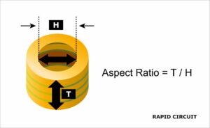
- Aspect Ratio
What is the aspect ratio in the PCB industry?
The aspect ratio is the thickness of a PCB divided by the diameter size of a drilled hole In PCB fabrication.
The aspect ratio is an important parameter for a plating process. Hole sizes that are small compared to board thickness may result in unsatisfactory plating or open holes. Plating must flow through the hole properly to achieve acceptable copper plating.
The bigger the aspect ratio, the more difficult it is to achieve reliable plating.
For the 10:1 Aspect Ratio,
If the board thickness is 1.6mm, the hole size must be >=0.16mm
If the board thickness is 2.0mm, the hole size must be >=0.20mm
If the board thickness is 3.0mm, the hole size must be >=0.30mm
- Bare Board: The term describes a circuit board that has no components mounted on it.
- BOM (Bill of Materials):
In PCB manufacturing and designing, a Bill of Materials (BOM) is a detailed list of all components, materials, and quantities needed to assemble a printed circuit board. It includes vital information like part numbers, descriptions, and specifications for each component used in the design and production process.
The Bill of Materials (BOM) is a critical document in both PCB designing and manufacturing. During the design phase, the BOM outlines all the components required to implement the circuit, ensuring the design can be accurately translated into a physical board. In manufacturing, the BOM helps coordinate the sourcing and assembly of parts, providing detailed data on the component type, value, and supplier. A well-structured BOM ensures that both the design and production processes run smoothly, reducing the likelihood of errors, delays, or missing parts.
- Glass Transition Temperature (Tg) :
In PCB laminates, Tg stands for Glass Transition Temperature. It is the temperature at which the material transitions from a rigid, glassy state to a more flexible, rubbery state. Tg is a critical property because it affects the mechanical stability, thermal reliability, and performance of the PCB in high-temperature environments. PCB material is hard and brittle Below Tg and material becomes soft and flexible above Tg.
- High-Tg Materials: Laminates like FR4 with a higher Tg can withstand higher operating temperatures, making them ideal for high-temperature applications like automotive, aerospace, and industrial electronics.
- Standard Tg Values: Typical Tg values for PCB laminates range from 130°C to 170°C, but high-Tg materials can exceed 170°C.
- Design Rule Check (DRC): DRC is a verification process that ensures a PCB design adheres to specific manufacturing constraints and electrical requirements. It helps identify potential issues before fabrication, reducing errors and rework.
Design for Manufacturability (DFM): DFM refers to designing PCBs with manufacturing capabilities and limitations in mind. It ensures that the design can be produced efficiently, cost-effectively, and with high quality.
