Products
PCB Products:
Introduction
When it comes to printed circuit boards (PCBs), single layer PCB and double layer PCB are two of the most common types used in electronics manufacturing. Choosing the right PCB type is crucial for optimizing your project’s performance, cost, and complexity. In this article, we’ll explore what single layer and double layer PCBs are, their advantages, disadvantages, and typical applications to help you make an informed decision.
What is a Single Layer PCB?
A single layer PCB is the simplest type of printed circuit board. It consists of a single layer of conductive material, usually copper, laminated on one side of a non-conductive substrate. Electronic components are soldered on the opposite side of the copper layer, and the circuits are routed only on one side.
Key Features of Single Layer PCB
- Single conductive layer: Copper traces are present only on one side.
- Simple design: Easy to manufacture and repair.
- Cost-effective: Ideal for low-cost electronics.
- Limited complexity: Suitable for basic circuit layouts.
Common Applications of Single Layer PCBs
- Consumer electronics (calculators, radios)
- Power supplies
- LED lighting systems
- Simple sensors and controllers
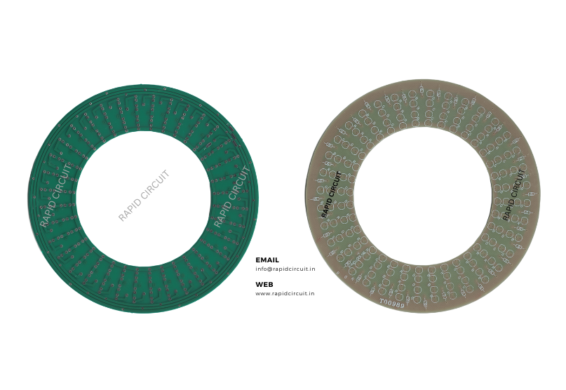
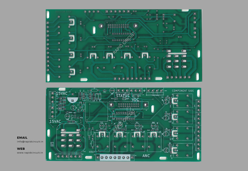
What is a Double Layer PCB?
A double layer PCB contains two layers of conductive copper, one on each side of the insulating substrate. This allows more complex circuit designs by enabling connections on both sides, linked via vias (small plated holes).
Key Features of Double Layer PCB
- Two conductive layers: Copper traces on both sides of the board.
- Increased circuit density: Allows for more complex and compact designs.
- Better electrical performance: Reduced circuit size and improved signal integrity.
- Moderate cost: Slightly more expensive than single layer PCBs due to added complexity.
Common Applications of Double Layer PCBs
- Industrial controls
- Power amplifiers
- Automotive electronics
- Complex sensors and communication devices
Single Layer PCB vs Double Layer PCB: Main Differences
| Feature | Single Layer PCB | Double Layer PCB |
|---|---|---|
| Number of Copper Layers | One | Two |
| Complexity | Low | Moderate |
| Cost | Lower | Higher |
| Circuit Density | Limited | Higher |
| Size of Board | Larger for same circuit | Smaller and more compact |
| Electrical Performance | Basic | Improved |
| Manufacturing Difficulty | Simple | Moderate |
How to Choose Between Single Layer and Double Layer PCB?
Consider Your Project Requirements
- Budget: Single layer PCBs are cheaper and suitable for simple designs.
- Complexity: For intricate circuit layouts and higher component density, double layer PCBs are preferred.
- Performance: Double layer PCBs offer better electrical performance and signal integrity.
- Space Constraints: When size is critical, double layer PCBs allow compact designs.
Ask Yourself:
- Is your project simple or complex?
- How much space do you have on your PCB?
- What is your budget for PCB manufacturing?
- Do you need better electrical performance?
Advantages of Single Layer PCB
- Cost-effective and easy to manufacture.
- Simplified troubleshooting and repair.
- Perfect for straightforward electronic circuits.
Advantages of Double Layer PCB
- Supports complex circuit designs.
- Higher reliability and signal quality.
- Enables compact and lightweight devices.
Conclusion
Both single layer PCB and double layer PCB have their unique strengths. Selecting the right PCB type depends largely on your project’s complexity, budget, and performance needs. For basic applications, a single layer PCB suffices, while double layer PCBs are ideal for advanced and space-constrained designs.
Ready to design your PCB? Whether you need a simple single layer or a complex double layer PCB, consult a trusted PCB manufacturer to bring your electronics projects to life!